


The 4 Most Common Chip Bonding Methods in Semiconductor Packaging
- Sophia
- 5 days ago
- 3 min read
Featuring ALN, CuW, and Chip Submount Solutions
Chip bonding is a core process in semiconductor packaging — it physically and electrically connects a bare die to the substrate, ensuring performance, thermal management, and reliability. Various bonding techniques are used depending on the packaging application, and the selection of materials like ALN submounts, CuW submounts, and Diamond submounts plays a major role in supporting high-density wire bonding and heat dissipation.
Let’s break down the four major chip bonding technologies and how modern submounts are enhancing each one
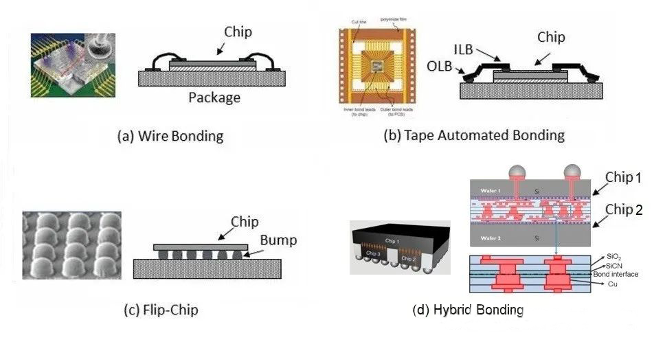
1. Wire Bonding — Reliable and Widely Used
Wire bonding remains one of the most traditional and widely adopted bonding methods. It uses fine metal wires (gold, aluminum, or copper) to connect the die to the lead frame or PCB. The bonding pads are typically located along the chip edges, and the bonding wires are encapsulated for protection.
Common Submount Materials:
Chip Submount: Provides mechanical support and bonding surface.
ALN Submount (Aluminum Nitride): Offers high thermal conductivity, ideal for heat-sensitive components.
CuW Submount (Copper Tungsten): Combines high strength and thermal stability, suitable for high-power applications.
Process Flow:
Equipment preheat and parameter setup
Wire feeding (gold, copper, aluminum)
Ball bonding or wedge bonding (using pressure, heat, or ultrasonic energy)
Inspection
Wire bonding is mature and cost-effective, but the increasing demand for compact, high-performance devices is pushing the industry toward more advanced techniques.

2. Flip Chip Bonding — High I/O Density, Better Signal Integrity
Flip chip bonding flips the chip face-down so that the bumps (tiny solder balls) directly connect to the substrate. It uses RDL (Redistribution Layer) to achieve a full-area (array) I/O layout, unlike the edge-limited wire bonding.
Key Benefits:
Higher I/O density per unit area
Shorter interconnect path → improved signal integrity
Chip backside is exposed → allows direct heatsink attachment via ALN or CuW submounts for efficient thermal dissipation
This makes flip chip bonding ideal for high-frequency and high-power devices. However, challenges like warping during reflow soldering or solder bridging between pads require precision engineering and high-reliability materials.

3. TAB (Tape Automated Bonding) — Flexible, High-Speed Assembly
TAB bonding mounts the chip on a flexible polyimide tape with pre-patterned copper leads. This technique enables automated mass production and is suitable for devices requiring fine-pitch interconnects — like LCD driver ICs or COF (Chip-On-Film) packages.
Process Highlights:
ILB (Inner Lead Bonding): Connects chip pads to tape leads via heat or ultrasonic bonding
OLB (Outer Lead Bonding): Aligns and bonds the tape to the PCB or substrate
Encapsulation or molding for protection
Using flexible substrates, TAB allows thin, lightweight package profiles. However, it has higher initial costs and tight process requirements, so it's best suited for high-volume production.

4. Hybrid Bonding — The Future of 3D IC Integration
Hybrid bonding combines both metal-to-metal (Cu-Cu) and dielectric-to-dielectric (oxide-to-oxide) bonding for ultra-fine interconnect pitches — even below 1 µm. It’s the leading choice for 3D memory stacking and heterogeneous integration.
Advantages:
Up to 10,000x I/O density vs traditional micro-bumps
Lower inductance, capacitance, and resistance → faster signal, lower power
Enables wafer-to-wafer and die-to-wafer bonding
Perfect for high-performance computing (HPC) and AI applications
Submount Relevance:
Even in hybrid bonding, chip submounts play a role during intermediate testing, temporary support, or heat dissipation during processing.

Summary
Each bonding method offers unique advantages:
Bonding Method | I/O Density | Thermal Mgmt | Automation | Suitable Submounts |
Wire Bonding | Low–Medium | Moderate | High | Chip, ALN, CuW Submount |
Flip Chip | High | High (with submount heatsink) | Medium | ALN Submount, CuW Submount |
TAB | High | Good | Very High | Flexible films, Chip Submount |
Hybrid Bonding | Ultra High | High | Medium | Temporary Chip Submount |
In all these bonding workflows, submounts — especially ALN, CuW, and custom chip submounts — provide the physical support and thermal performance needed for reliable wire bonding and beyond.
Looking for High-Performance Submounts?
Whether you’re developing wire-bonded laser chips, high-frequency RF devices, or 3D-stacked memory, choosing the right submount solution is critical. ALN submounts, CuW submounts, Diamond submounts are ideal for thermal conductivity and mechanical strength and provide custom flexibility for advanced bonding processes.
Let’s connect and find the best submount for your bonding application.
Comments